[INQ. NO. 2212E21] Established in 2000, ENF Technology specializes in the production of electronic materials and fine chemicals. The company has become a pioneer in the electronic materials industry by developing technologies and tackling new challenges through business diversification and constant R&D.
As a result, ENF Technology has achieved remarkable sales growth and are preparing for the next leap.
Based on distinctive technologies in the field of electronic materials, ENF Technology’s market share in process chemicals, fine chemicals, and color pastes is also growing fast.
Expanding its business in new areas, ENF Technology has been striving to become a leader in the global electronic materials market. To cope with the expanding demand of the semiconductor market in the US, ENF Technology established a new plant in Kyle, TX in 2021.
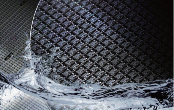
Ultra-pure Ammonia Hydroxide(NH4OH) for cutting-edge semiconductor manufacturing process
ENF Technology manufactures the highest purity ammonia hydroxide in the world. Ammonia solution is an essential agent used in the cleaning and etching process in the semiconductors industry.
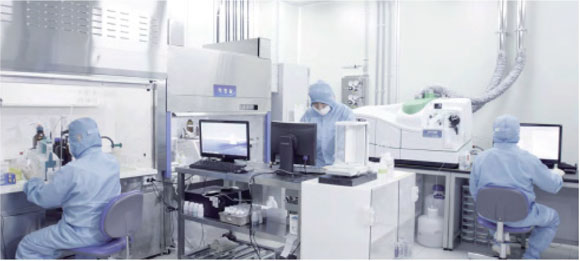
The new plant in Kyle, TX is equipped with cutting-edge manufacturing facilities including best-in-class quality analysis and management systems to provide reliable supply and consistent product quality.
To meet and exceed the ever-increasing purity requirements for next-generation semiconductor technology, ENF Technology is capable of analyzing the material at the level of 1 PPT metal levels, manufacturing the highest-quality de-ionized water (DIW), and controlling 0.1 µm particles by applying the hyperfine filters to manufacture ultra-pure ammonia hydroxide.
Stripper (Cu PERR)
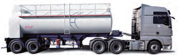
ENF Kyle plant manufactures a stripper that mainly removes the residue from the Cu-etching stage in the semiconductor manufacturing process.
ENF Technology was able to manufacture and distribute the stripper solution (which was developed by its R&D at the headquarters) from its plant in Texas, based on the formulation, additives application, and purification technologies.
korean-electronics.com | Blog Magazine of korean electronics, brands and Goods
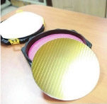 BECS has developed a liquid-type coating for wafer back grinding that can replace the existing lamination film type. The wafer back grinding is a process to reduce resistance and improve heat conductivity by removing needless films and grinding the thick reverse side. Consisting of film type and liquid type, it reduces over 70% material costs compared with BG tape. The wafer back grinding can be applied to the process of dicing before grinding (DBG) and stealth dicing before grinding (SDBG). Back grinding is easy for the sawing process and minimizes the package thickness as well as exhales working heat. The liquid coating reduces over 70% material costs compared with BG tape. The process is as simple as four to six steps.
 In the process of laser sawing, it forms a protective film on the surface of the wafer to be cut, which protects the wafer from debris and particles generated while dicing. The coating agent is released in the shape of film when it is dipped into water after use. The amount of yielding wafer dicing increases by preventing cracks on the wafer that may be created during the sawing process. It is also easy to release in the shape of film or tape in the water and dries quickly.
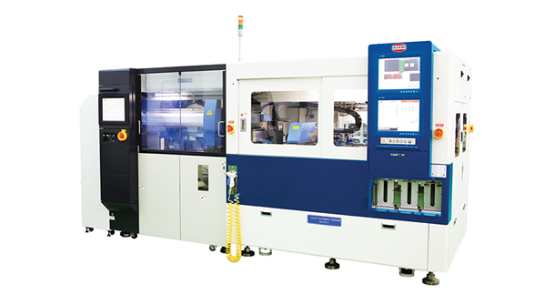
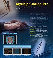 The progress of electronic systems may start from designing. Engineers are very aware of it and use software tools at the initial stage of production. One of the most useful tools is MyCAD, a widely popular electronic design automation software. Recognizing all of these conditions, Korea’s SELOCO is taking responsibility when it comes to providing cost-effective and innovative design tools.
 In cooperation with a few major global foundries, SELOCO is involved in ASIC & SOC business in order to develop the non-memory semiconductor business, and offer MPW (Multi-Project Wafer) service and various foundry services. Main foundry companies are EPISIL, HHNEC, VIS, UMC, SMIC, and ASMC. Regarding ASIC service, SELOCO works closely with your staff to offer full-custom chip design implementation from design proposal, IP design, configuration, chip level integration, FPGA validation, etc. For more information, you can find at seloco.net/main/intro.html.