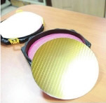
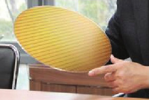
 The price of a single semiconductor wafer the size of two hand palms is extremely costly for the surface is coated with gold. A wafer of 750 micrometer thickness is polished to thinner than one-third through ultra-high-speed back grinding. In this process, even a slight difference in thickness may cause a problem in which electricity does not travel across chips. This is why the role of the back grinding tape holding the wafer is critical in the process of grinding.
Since its establishment in 2006, BECS Co., Ltd. has developed a liquid masking coating agent by utilizing the know-how gained through its clearing business in the semiconductor and fl at panel display (FPD) fields in the early stage. The company further transformed itself from a total cleaning solution provider to a fine chemistry company and successfully sett led the masking coating business, a core process of semiconductors, LCDs, and TSPs in the market.
PRM 1100; Wafer Back Grinding Lamination Film
 BECS has developed a liquid-type coating for wafer back grinding that can replace the existing lamination film type. The wafer back grinding is a process to reduce resistance and improve heat conductivity by removing needless films and grinding the thick reverse side. Consisting of film type and liquid type, it reduces over 70% material costs compared with BG tape. The wafer back grinding can be applied to the process of dicing before grinding (DBG) and stealth dicing before grinding (SDBG). Back grinding is easy for the sawing process and minimizes the package thickness as well as exhales working heat. The liquid coating reduces over 70% material costs compared with BG tape. The process is as simple as four to six steps.
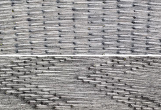
Dicing Before Grinding (DBG)
If the wheel keeps rotating with die separated, faults may occur due to the collision among chips and mixed dust. As kerf width is maintained between dies, chips are fixed during back grounding. It is easy to release with no residue.
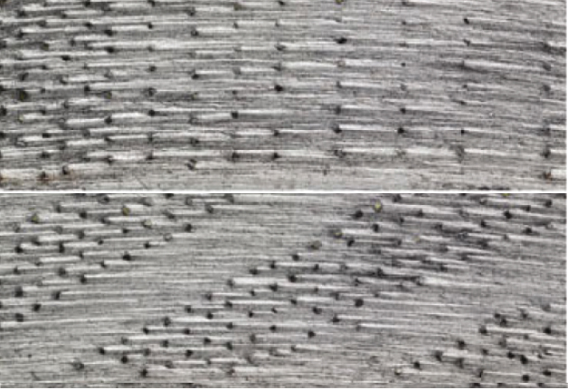
Stealth Dicing Before Grinding (SDBG)
 In the process of laser sawing, it forms a protective film on the surface of the wafer to be cut, which protects the wafer from debris and particles generated while dicing. The coating agent is released in the shape of film when it is dipped into water after use. The amount of yielding wafer dicing increases by preventing cracks on the wafer that may be created during the sawing process. It is also easy to release in the shape of film or tape in the water and dries quickly.
korean-electronics.com | Blog Magazine of korean electronics, brands and Goods

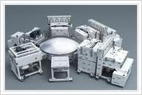
 Sang-a Frontec specializes in secondary batteries and equipment and components for LCDs, office automation systems, and semiconductors. The company’s core business is engineered plastics and fluoride polymers, which are used to manufacture a wide range of components and materials for products as well as production equipment. The company’s major products include LCD