PCB Matching Platform System

https://korean-electronics.com//inquiry
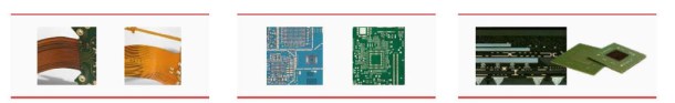
Cheese PCB is a PCB matching platform that connects someone who wants to have PCB with a PDB manufacturer. In this process, first, someone who wants to have PCB needs to upload the data on manufacturing of PCB into Cheese PCB. Next, many manufacturers who want to manufacture PCB signal their intent to manufacture the PCB by presenting the price level and manufacturing schedule they each want.
The client for PCB selects the manufacturer who presents ideally the price, quality, and schedule for the client among the many examples presented for matching. This system is the first materialized in the world and is worthy of being called a new PCB manufacturing platform that leads new paradigm in that field. With this PCB matching platform, both client and manufacturer can thus benefit.
Through this convenient one-stop process, the client for PCB can receive more advantages among many conditions from many manufacturers and the manufacturer can select a model that best suits its technology level and schedule.
Moreover, Cheese PCB leads to structural changes in the sales environment from the existing consumptive offline sales into new online sales, and thus greatly contributes to the profit model improvement of each manufacturer.

korean-electronics.com | Blog Magazine of korean electronics, brands and Goods

Vacuum Hot Press

https://korean-electronics.com//inquiryFusei Menix was founded in 1983, and engaged in the oil press sector with global technological competitiveness in the semiconductor & PCB equipment field. Fusei Menix passed the national project on technology innovation in 2007, and recognition of technology from the government such as winning the Korean world-class product award 2010.
Fusei Menix invented new systems such as the 5-RAM system and vacuum hot press through continuous research and development. It has gained a good reputation for quality and energy-saving among its worldwide customers. It has also won domestic and international recognition for its technology.
Therefore, the maker recorded in the best sales earning and was awarded the president’s citation in 2010. It has successfully performed a national project on laminating methods during 2011~2019, and obtained certifications such as ISO9001, CE Mark, KCS and other safety and quality certifications, and is in the process of obtaining ISO14001 and Green Mark certification. Fusei Menix is striving to expand its presence in overseas markets such as China, ASEAN, Japan, the USA, and Russia by continually developing eco-friendly and hi-tech products.
Fusei Menix’s vacuum hot press is its cutting edge technology, and has been recognized for quality by many customers. Fusei’s high quality vacuum hot press is applied to many fields of PCB like rigid PCB, flexible PCB, package substrate, MLB, HDI and special PCB such as metal PCB and ceramic PCB.
Many companies, domestic and overseas, like SAMSUNG, LG, DAEDUCK, SIMMTECH, YPG, BH, KINSUS, FOXCONN, MEKTRON, MULTEK and SUMITOMO are using Fusei’s highquality vacuum hot press and recognizing Fusei’s superior quality and technologies especially, high-quality pressing, vacuum and temperature control. Fusei’s VHP is standard in domestic markets and expanding worldwide. Now the maker is developing vacuum hot press for energy saving and Press for high temperature.
Fusei Menix’s high-quality transfer molding press is applied to many fields of semiconductors and LED. Any companies, domestic and overseas, like SAMSUNG, LG, ASE, ONSEMI, COMPEQ INFINEON, IXYS, SP Semiconductor, SHINDENKEN, AUK, FAGOR, and NMB are using Fusei’s high-quality transfer molding press and recognizing Fusei’s superior quality and technologies. Fusei’s TMP is standard standard in domestic markets and expanding worldwide.

korean-electronics.com | Blog Magazine of korean electronics, brands and Goods

Ink, OCA & OCR Removers from Glass Panels

https://korean-electronics.com//inquiryThese removers are a specially designed solution to remove OCA, OCR and other inks from the glass surface for reusing the glass panels, causing no damage to the glass panels. For removal, a simple method is available and easy to use.
The user needs to heat the removing solution up to 70~90 degrees or so. The best temperature can be found by a prior test. Dipping the glass panels in the solution for about 2~10min. is also required. The best dipping time shall be decided by the prior test. After fully removing the inks, the user needs to take out the glass panels, wash with warm water, and dry.
Remover series products are developed by each customertailored style, not by ready-made, so that the chemical can give the best efficiency in accordance with each customer’s different working conditions, various materials, etc.


Cleaners for Electronic & Other Materials

These cleaners are eco-friendly, low-toxicity, and powerful cleaners. They can easily remove pollutants from various substrates. No discoloration of substrates exists and natural drying is possible. It is required for the user to heat up the removing solution up to 50 degrees or so. Dipping the glass panels in the solution for about 5min. is also required. The best working condition shall be decided by the prior test.
Cleaner series products shall be developed by each customer-tailored style, not by ready-made, so that the chemical can give the best efficiency in accordance with each customer’s different materials to be cleaned.
Established in 1995, Sechang Chemical Co., Ltd. has aimed at improving both the manufacturing technology and the product quality of the Korean PCB Industry, by bringing in and developing the application of both high and new technology for the chemicals and ink products used for the manufacture of PCB and PCM products. Focusing on the needs of its customers, it expanded its product range.
Based on the mutual firm trust accumulated over more than 20 years, Sechang Chemical has started to produce various chemical products for PCB manufacturing under a technical partnership with RBP Chemical Technology, who are one of the worldwide companies developing newer and higher technology to produce higher quality products. Thanks to this new system of local production, it has strengthened its capability to meet customers’ requirements for new products for their own specific working environment. Additionally local production also allows the company to offer more competitive prices.
Thanks to the successful business newly established from the late 1990s for Coates Circuit Products (Sun Chemical), who is one of the world leading companies in the industry as the first developer for solder masks, the first company to acquire ISO14001 certification in that industry and also the world largest ink manufacturer, Sechang Chemical could also form the basis of its new ink business to meet its customers’ continuous demands for higher quality, higher yield and environment-friendly products for PCBs.

korean-electronics.com | Blog Magazine of korean electronics, brands and Goods

PCB Equipment

https://korean-electronics.com//inquiryEstablished in 2011, Changsung Corporation has positioned itself as a professional in South Korea in the field of PCB equipment. Changsung specializes in manufacturing equipment for semiconductors, FPD, PCB, solar, and automation based on its brilliant various core technologies.


Vertical Stripper

Changsung’s vertical stripper, a kind of PCB device, removes cured dry film by vertically converting the PCB substrate.
This vertical stripper loads a PCB (Printed Circuit Board) into the loading part, converts it vertically, and makes it move into the strip zone. And then the vertical stripper applies chemical for stripping and removes dry film.
After stripping, this vertical stripper converts the PCB horizontally again at the unloading part after cleaning and drying, and then PCB is exposed. As PCB is transferred in the loaded condition, PCB is free from contact problems and thus guarantees superior quality of PCB. The entire transferring method is controlled by an automatic robot system.


Vertical Developer

Changsung’s vertical developer develops by converting the PCB substrate vertically and separating the exposed part and the unexposed part from the ultraviolet rays.
This vertical stripper loads the PCB into the loading part, converts it vertically, and makes it move into the develop zone. And then the vertical developer applies chemicals and develops. After the developing process, this vertical developer converts the PCB horizontally again at the unloading part after cleaning and drying, and then the PCB is exposed.
As PCB is transferred with the loaded condition, PCB is free from contact problems and thus guarantees superior quality of PCB. The entire transferring method is controlled by an automatic robot system.
Since its founding in 2011, Changsung Corporation has set itself a goal of becoming a ‘Global Hidden Champion’ to constantly strive to improve technology innovation, as well as improving customer value through differentiated manufacturing technology and new technology development in the rapidly changing domestic and international industrial structures. Changsung will strive for perfect innovative quality by seeking better value and satisfaction of its customers.

korean-electronics.com | Blog Magazine of korean electronics, brands and Goods

PCB Surface Treatment Using Chemical Materials

https://korean-electronics.com//inquiryYMT Co., Ltd. has recorded steady growth in the fields of electronics & chemical materials, based on its slogan of “Create a Better World through Technology.” YMT is boosting its solid presence both domestically and in the overseas market in the rapidly changing electronic field, while developing new products that customers want with maximum investment in technology development.
Among the company’s various capabilities, its basic competence is in the surface treatment for PCB using chemical materials. The surface treatment using chemical materials is so necessary for preventing parts from oxidizing and is widely applied not only in PCB, semiconductor packages, general semiconductors, and also in plastics.
In particular, the company currently possesses the world’s highest level of technologies related to gold plating and copper plating.
Currently, YMT has developed electronics materials and semiconductor chemicals materials and is proceeding with new business. While the existing Japanese-made products form the copper surface with this type of electric copper plating, YMT adopts the way of electroless chemical copper plating, an integrated technology of its know-how regarding technology of copper-plating chemical materials and thus forms an ultra-thin copper foil by plating copper on the surface of the aluminum carrier.
This was a remarkable accomplishment whereby YMT advanced into market dominated by Japanese-made products with its own technologies without infringing patents they hold. Compared to electric copper-plating, YMT’s electroless chemical copper-plating features regular surface thickness of an ultra-thin copper foil, and it can thus be applied to high-end products requiring high reliability. Moreover, this technique of electroless chemical copper plating leads to comparatively high price competitiveness compared to the Japanese way of electric copper-plating because of its excellent cost structure.
Through these various attempts for development, YMT is actively responding to the prospect of future new products and the trend change of electronic industry and thereby preparing for advancing not only into the PCB industry, but also into postprocessing of semiconductor, etc. YMT is thus elevating its global presence significantly.

korean-electronics.com | Blog Magazine of korean electronics, brands and Goods

PCB Total Chemical Solutions

https://korean-electronics.com//inquirySince the beginning of the 1960s, the PCB industry has grown into a core component industry in Korea. Over the past 50 years, Korea has overcome many trials and failures, raising its status as a PCB industry powerhouse.
ORCHEM, which was established in 1991 and has grown along with the domestic PCB industry, developed the world’s first ion type and colloid type process solutions with its own technology in the horizontal electroless chemical copper process in 2013. By successfully applying mass production to major PCB makers, the company is able to further improve its industrial competitiveness.
In addition, in line with the high-tech trends that the PCB industry is aiming for, ORCHEM has established a foundation for strengthening the collaboration system with customers by securing the best technology for SAP/MSAP processes and transferring to a new office building equipped with advanced research facilities in 2017.
ORCHEM is the only PCB total chemical maker in Korea and will be your best partner in the PCB industry, opening the future together with its customers. Appreciating the long trust and loyalty from its customers, ORCHEM is committed to rewarding them with the best quality and service.

korean-electronics.com | Blog Magazine of korean electronics, brands and Goods

Soldering Robot & Soldering Irons

https://korean-electronics.com//inquiryExso Corp., ltd. was established in 1978 as the nation’s first specialized company for soldering iron and PCB-related equipment.
The products from the company are being exported to more than 30 nations, being recognized as the both nominally and virtually global top brand. The steady investment in R&D has naturally resulted in accumulated brand awareness in global markets. As all of its products from commercial soldering iron to PCB-related equipment to peripherals were produced with strict process of quality management, any clients can use them in full trust.


Desktop 4-axis Soldering Robot (AutoRo-5634)

This soldering robot is designed to be used in various facilities at a reasonable price and is economical. Regardless of location and position, this as a tabletop equipment is easy to install. This adopts a high-frequency and high-efficiency mode (direct heating). The heating method can be applied to select for the job. The convenient one-touch indutip in turn benefits the workability in replacement schemes. A drilling method has been applied to the system for shatterproof protection.
This can be applied to various products and soldering temperature can be freely set. As it can adjust the soldering iron unit in different directions, you can prevent the PCB and component damage. Numerical control is available in setting temperature (room temperature conditions: ± 1˚C). With portable LCD teaching pendant, the programming is simple and easy to learn. In the soldering process, solder tip has a fast heat recovery and long life.


Pistol-type Wireless Soldering Iron (EX-376G)

This wireless soldering iron has an excellent portability with rechargeable soldering iron. It is possible to shorten the working time by fast preheating time of 20 seconds. The high performance of maximum 420˚C enables soldering at high temperatures. This can be used continuously for two hours after one charge. The front LED lamp enables work in dark place. The ergonomic design allows the user to operate easily.


Rechargeable Wireless Soldering Iron (EX-376)

This has an excellent portability with rechargeable soldering iron. It is possible to shorten the working time by fast preheating time of 20 seconds. The high performance of maximum 420˚C enables soldering at high temperatures. This can be used continuously for two hours after one charge. As it is designed as stand-type, storing operation is easy and convenient working environment is ensured. The front LED lamp enables work in dark place. This equipment is also designed in consideration of ergonomic merit, and thus allowing the user to operate easily.


korean-electronics.com | Blog Magazine of korean electronics, brands and Goods

Deep Learning Machine Vision Solutions

https://korean-electronics.com//inquirySUALAB is a leading provider of deep learning machine vision solutions. SUALAB, home of excellent engineers from deep learning and machine vision fields, combines the technologies of those industries to develop products that provide more convenience to people’s daily lives.
In particular, SUALAB enables fast and accurate machine vision inspection by using deep learning algorithms and image analysis technologies.
This solution, ‘SuaKIT’, is applicable in various manufacturing industries such as electronics (display, PCB, semiconductors, batteries, etc.), automotives, and others where existing machine vision technology is not easily implemented.


Deep-learning S/W Library for Machine Vision ‘SuaKIT’

SuaKIT accurately detects position, area, and shape of the defects in the unit of pixels. It classifies multiple images in line with predetermined classes. This solution detects, and classifies various types of objects in a single image in a box form.
The company’s president explained, “In line with 4th industrial revolution era, the demand for factory automation solutions in the near future is expected to increase, and so we decided to pioneer a new market for us where big strides so far had not been made through existing technologies –by utilizing our differentiated technologies.”
SUALAB has successfully commercialized solutions for various kinds of manufacturers including Samsung, POSCO, Kolon, Korea Minting and Security Printing Corporation, etc. – based upon its own differentiated AI technologies. SUALAB was selected as a global top-8 start-up in Asia’s only machine vision area in 2016 by the AIA, the largest global machine vision association, in recognition of such performance.
SUALAB was also awarded the grand prize in the machine vision section at the ‘2018 Industry Awards Korea,’ where the company was recognized for creating new value by developing technology related to the manufacturing industry. And early this year, SUALAB participated in a global business meeting where global business issues were dealt with between a BMW official and nine domestic start-ups hoping to advance into overseas markets in both vehicle (AI, sensors, and autonomous driving, etc.) and convergence areas (braille skills, new materials, manufacturing process).

A spokesperson for the company raised expectations by saying “Cooperation with a multinational company offers an invaluable opportunity for start-ups to scale-up, so through this we will aggressively proceed with investment inducement, pioneering overseas sales opportunities.”


korean-electronics.com | Blog Magazine of korean electronics, brands and Goods

Surface Treatment and Processing of Pless Plates

https://korean-electronics.com//inquirySungsan High Tech was established in 2000 and has been engaged in the surface treatment and processing of pless plates for forming centering on SUS plates that are used for lamination such as the SUS plate for CCL, MASSLAM, MLB, FPCB, etc. and also jigs and fixtures.
Sungsan High Tech has so far made great efforts to develop technologies required for processing various types of plates and for surface treatment and processing and secured the quality winning trust of many customers, which enabled it to continuously supply its products to professional PCB companies.
While a variety of PCB materials including those that are used for electronic products such as computers and smartphones, it has made enormous efforts to localize the SUS plate, which had depended on imports for 30 years, and in response to customer demands for quality specification and precision and also made efforts to enhance quality and reduce costs by combining new materials and production.
Currently, Sungsan High Tech is locally supplying parts that PCB companies need when entering overseas markets. Also, it has made efforts since 2017 to localize some of the SUS plates that had depended on imports for 30 years, and as a result it successfully localized SUS plate301 for the first time in South Korea in the beginning of 2018 and began to sell the plate to domestic and foreign (Chinese) PCB companies.
The localized SUS plate is at least 30% less expensive than the imports and can be quickly delivered within two months, whereas imports from Japan currently take around ten months. This increases competitiveness and expansion in domestic and overseas markets is expected.
Sungsan High Tech has delivered its products to more than 100 domestic companies including professional PCB production companies, Samsung Electromechanics Co.,Ltd., Dae Duck Electronics Co., Ltd., Doosan Corporation Electro- Materials, etc. Sungsan High Tech is steadily supplying its products to PCBspecialized companies thanks to the client companies’ accumulated trust in the quality of its products, as a result of its developing technologies required for various kinds of plate processing and its all-out efforts for developing of newer surface treatment methods. Currently, Sungsan High Tech is largely exporting to China, Vietnam, Singapore, and the Philippines.


korean-electronics.com | Blog Magazine of korean electronics, brands and Goods

Optical 3D Scanner

https://korean-electronics.com//inquiryFirst launched in 1995, the ATOS series of 3D scanners has been continually developed by utilizing state-of-the-art technology.
Today, optical 3D measuring technology and full-field surface measurement systems have become a standard tool within virtually all industries worldwide. ATOS systems are used to reduce development times, optimize production processes and, at the same time, improve process security.


Full-field Measurement

ATOS is a 3D coordinate measuring machine. The fast, non-contact, optical 3D scanners deliver a high-resolution point cloud which precisely describes free-form surfaces and primitives regardless of part sizes, surfaces, finishes, and geometries. ATOS provides three-dimensional measurement data and analysis for industrial components such as sheet metal parts, tools and dies, turbine blades, prototypes, injection molded parts, castings, and more.


Self-monitoring Systems

The high-resolution 3D scanners from the ATOS product line guarantee high process security. The proven stereo camera setup allows a completely self-monitoring system. Calibration and sensor movements are checked continuously preventing measuring errors and thus delivering accurate and reliable measuring data. The projection unit‘s narrowband Blue Light Technology enables precise measurements regardless of ambient light conditions.
Used in conjunction with GOM‘s professional inspection software, ATOS supplies full-field deviations from CAD, complete shape & dimension analyses, and comprehensive measurement & inspection reports.
ATOS 3D scanners are key elements of the entire process chain, from construction through to production and maintenance including shorter research and development times, faster production processes, and improved quality assurance within the entire lifecycle of the product.
Preset sensor models for different resolutions and measurement field sizes can be exchanged quickly and reliably. After the change, there is no need for re-calibration.
The projection technology developed by GOM operates with narrowband blue LED light. As a result, accurate measurements can be taken independently of ambient light conditions.
In ATOS Core, the two cameras are combined with the projector to capture three views of an object in a single measurement process. This requires fewer scans and delivers higher quality data – even on shiny and complex objects.
Thanks to the proven stereo camera setup, ATOS Core monitors its own activities. Calibration, transformation accuracy and component movements are subject to continuous control. This guarantees that the system generates reliable and precise measurement data.
Different software packages are available for ATOS Core. In GOM Scan, the focus is on 3D meshes, while ATOS Professional offers a broad range of functions for parametric inspection.
To enable quick and accurate component and fixture referencing, ATOS Core can be extended to include a photogrammetry option – with TRITOP for manual or ATOS Plus for automated applications.

korean-electronics.com | Blog Magazine of korean electronics, brands and Goods